

Fujifilm announced on May 21, 2026, that it will present advanced semiconductor packaging research, including PFAS-free PBO, at ECTC 2026 in Orlando, Florida, from May 26–29, 2026.
Fujifilm Unveils PFAS-Free PBO at Semiconductor Packaging Conference
Fujifilm Corporation revealed plans to showcase its latest advancements in semiconductor packaging technologies at the Electronic Components and Technology Conference (ECTC) 2026, including its PFAS-free polybenzoxazole (PBO) material. The event, scheduled for May 26–29, 2026, in Orlando, Florida, will feature technical presentations and product demonstrations by Fujifilm’s U.S.-based subsidiary, FUJIFILM Electronic Materials U.S.A., Inc.
The company’s research, developed in collaboration with imec, a global leader in nanoelectronics research, focuses on bonding technologies and interconnect formation processes for advanced packaging architectures, such as 2.xD and 3D designs and high-bandwidth memory (HBM). A key innovation highlighted is the Sn (tin) damascene process for fine-pitch microbumps, which Fujifilm and imec jointly developed to enable smaller, more efficient semiconductor components.
Sustainability Drive Underpins New Materials
Fujifilm emphasized its commitment to sustainability through the introduction of PFAS-free PBO, a material used in photosensitive insulating applications. Heather Mazjanis, vice president of Photopolymers at FUJIFILM Electronic Materials, U.S.A., Inc., stated,
“Fujifilm’s new PFAS-free PBO product shows Fujifilm’s ongoing commitment to sustainability and the environment. Fujifilm is also promoting PFAS-free photoresists used in various advanced technologies, further supporting responsible innovation.”
Heather Mazjanis, vice president, Photopolymers, GBD Core Photoresists and PBO, FUJIFILM Electronic Materials, U.S.A., Inc.
The PFAS-free initiative aligns with broader industry efforts to phase out per- and polyfluoroalkyl substances (PFAS), which have raised environmental and health concerns due to their persistence in ecosystems. Fujifilm’s shift reflects growing regulatory and consumer pressure on semiconductor manufacturers to adopt greener alternatives.
ECTC 2026: A Hub for Semiconductor Innovation
ECTC 2026, the world’s largest conference dedicated to semiconductor packaging technologies, will attract over 2,500 attendees, including scientists, engineers, and business leaders. Fujifilm will exhibit its ZEMATES™ product line of photosensitive insulating materials at Booth #1003, showcasing solutions for next-generation chip design and manufacturing.
The conference’s technical program will address challenges in miniaturization, thermal management, and interconnect reliability, critical for advancements in 5G, AI, and IoT devices. Fujifilm’s presentations will focus on enabling technologies for 3D packaging, which allows stacking of multiple chips to improve performance and reduce form factors.
Broader Implications for the Semiconductor Industry
Fujifilm’s research underscores the industry’s shift toward specialized materials and processes to meet demand for smaller, faster, and more energy-efficient semiconductors. The Sn damascene bonding process, for example, could reduce reliance on hybrid bonding techniques, which are costly and complex. Analysts note that such innovations are vital as global chip production faces bottlenecks in scaling advanced nodes below 5nm.
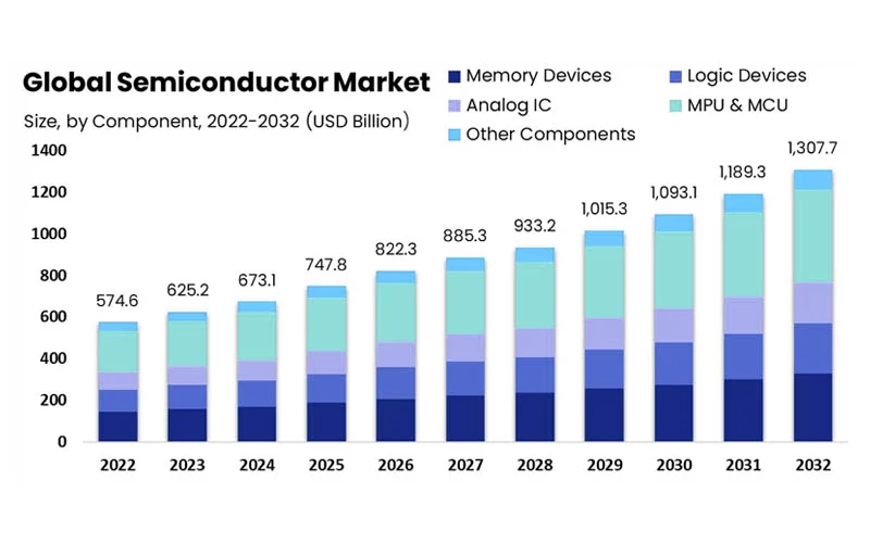
However, the transition to PFAS-free materials presents technical challenges, including maintaining performance benchmarks in high-temperature and high-humidity environments. Fujifilm’s success in this area could set a precedent for other suppliers, accelerating the adoption of sustainable practices across the supply chain.
What’s Next for Fujifilm’s Semiconductor Division?
Fujifilm’s participation in ECTC 2026 signals its intent to strengthen its position in the semiconductor materials market, where it competes with firms like JSR Corporation and Shin-Etsu Chemical. The company’s focus on sustainability and advanced packaging aligns with its broader strategy to diversify beyond traditional imaging and life sciences segments.
While the immediate impact of Fujifilm’s PFAS-free PBO remains to be seen, the company’s collaboration with imec and its presence at ECTC highlight its role in shaping the future of semiconductor manufacturing. Analysts will monitor whether the technology gains traction among major chipmakers, potentially influencing industry standards and regulatory frameworks.
